
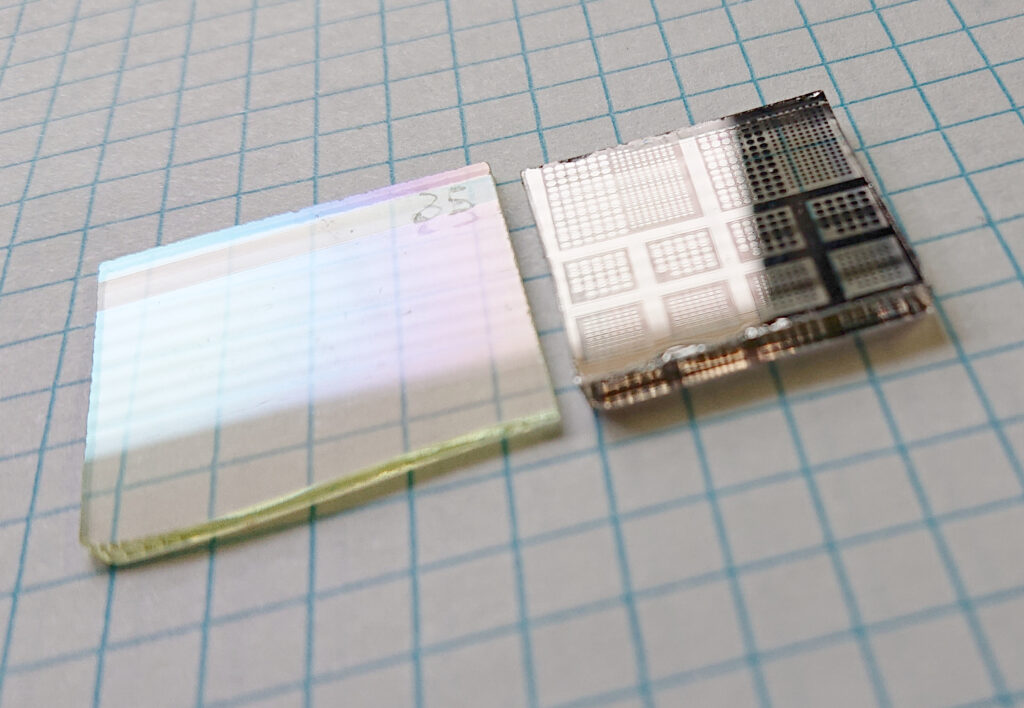
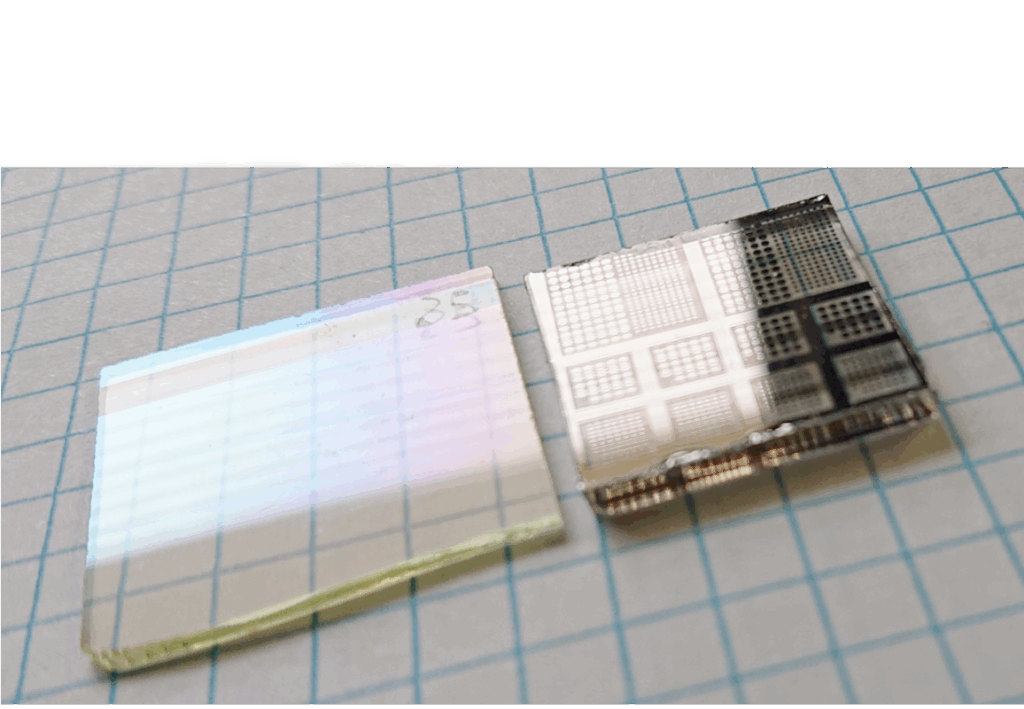
Zinc Oxide (ZnO) thin films are used in Dye Sensitized Solar Cells (DSSC) in LEDs and detectors. ZnO is a very forgiving material which displays its semiconducting properties when deposited in many different ways. For LEDs and Solar Cells, thin and uniform films are needed at least in parts of the device. DC or RF Magnetron Sputtering techniques give very thin and uniform films. Seen on the right in the image above the presence of the ZnO appear as this iridescent blue to red coating. Using sputtering again, a patterned NiV0.7 alloy is deposited to form metal/ semiconductor diodes.
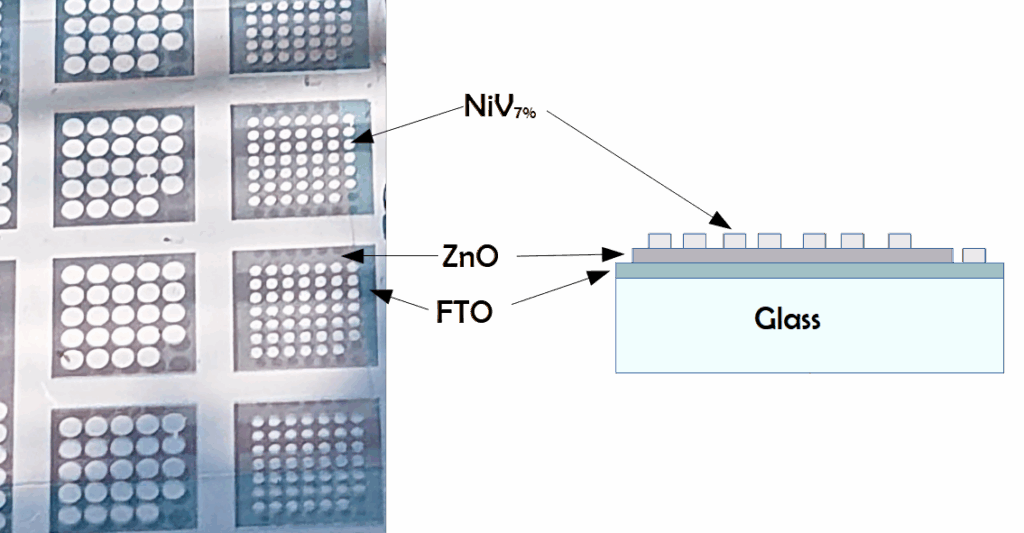
Device structure: The Schottky diodes are defined by the metal dots deposited. A close view of the device shows a red tinged area which is where the ZnO thin fim is located. Outside that area is the FTO film. Metal dots in that part of the device forms an ohmic contact with the degenerately doped FTO. Due to its extra high doping the FTO acts as a metal. Contacts made to that part of the surface shows a non-rectifying symmetric behavior although not perfectly linear as a true ohmic contact to a metal would be.
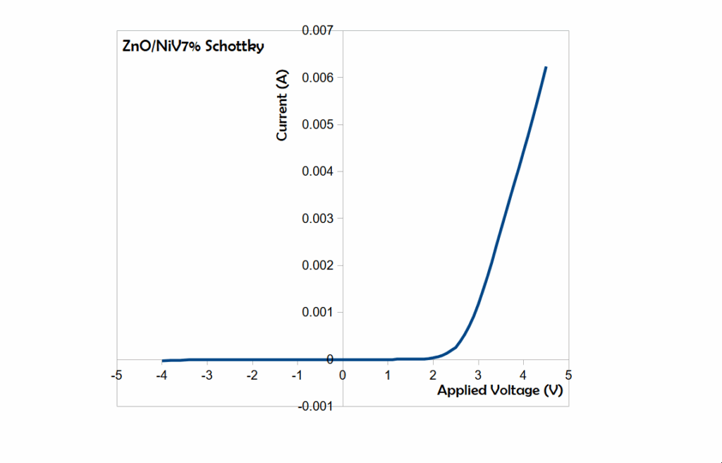
Current Voltage: In the above graph the current has been measured for voltages poing form -4V to 4V. the axes are linear and clearly show the rectifying behavior with high current of the positive bias side. An extrapolation of the ON curve give us a turn on of 2.5V approximately which is expected for a wide bandgap material like ZNO. The slope of the curve betrays the resistance of the device which is probably dominated by the resistance of the FTO layer.
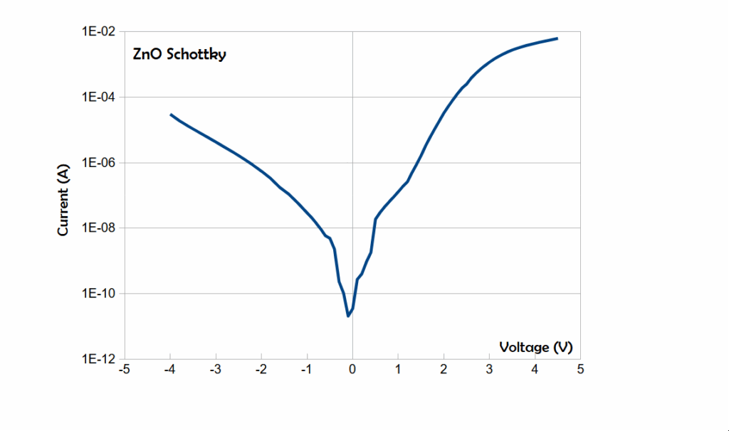
Reverse Leakage: The linear graph showed us the right relative proportion of the signals, but it can hide issues with the diode specially regarding leakage currents. In the semi-log graph above we have a better view of the lower reverse current and it is quite large especially for a wide bandgap material like ZnO.
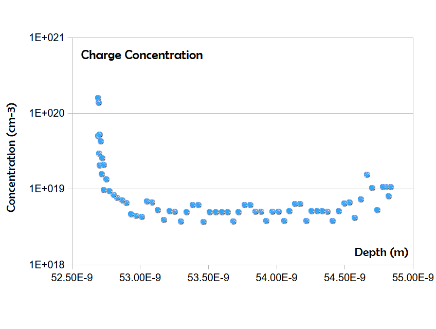
Carrier concentration: Measuring the capacitance voltage characteristics of our diode give us access to measuring the carrier concentration of the semiconductor. In this measurement we have to assume that the carrier concentration is constant to use the equations necessary to extract the profile, then if the extracted profile is indeed (relatively) constant we can trust the result. In this case A Keithley CV high frequency system was used. Due to the high leakage current only a small region between -4V and +2V of the characteristics could be measured. This limits the profile depth we can probe. A carrier concentration of 1019cm-3 is measured.
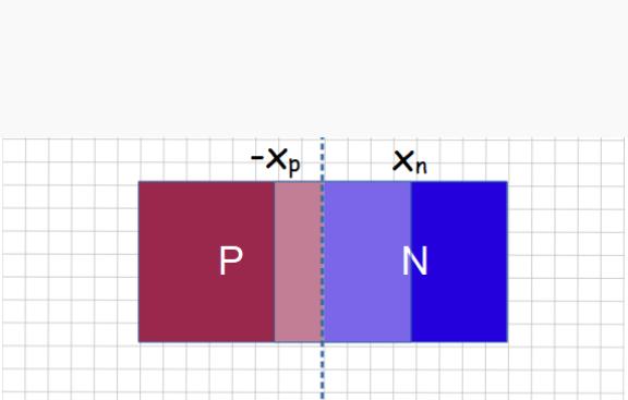
The high leakage can be a result of several things. The high carrier concentration result in very narrow depletion zone in reverse, reducing the value of the breakdown voltage. Thickness measurement on this sample using Rutherford backscattering have shown that the thickness of the device is approximately 100 nm, which means that the depletion zone will punch through if it extends beyond that leading to increased reverse current. This is by the way a method to make voltage controlling diodes although to my knowledge they are of the PN junction type.

Leave a Reply