
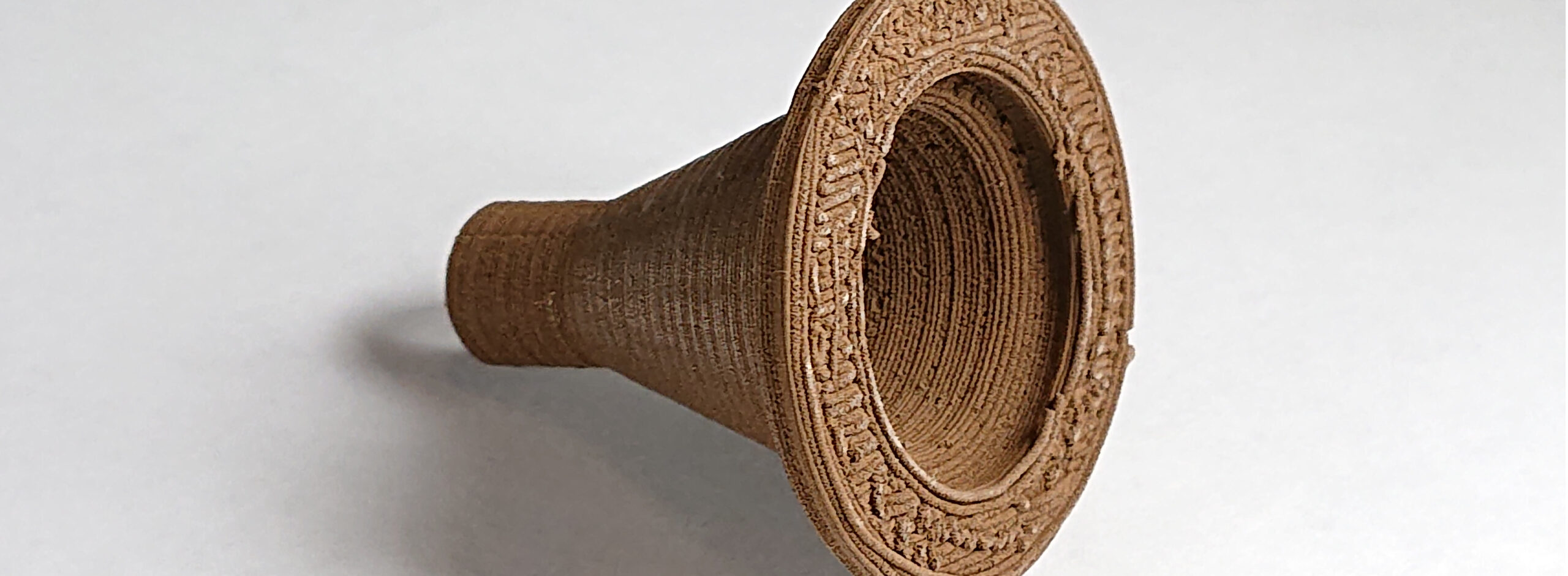
The advent of LEDs as lighting devices is the direct result of the invention of blue LEDs. This feat was achieved by Nichia in the mid-1990s using the GaN technology. Other technologies such SiC were experimented and saw a laboratory level success. Because of the size of the market for that kind of product and also the scientific and technical challenge is so interesting, a general race to the blue LED was started.
New technologies such as Organic LED saw a sustained effort tooting advantages such as low-cost ease of manufacture, ability to make large size devices and potential eco-friendliness. In that wave of effort ZnO was identified as a low cost environmentally friendly and sustainable wide bandgap material. Its bandgap is similar to that of GaN and therefore promises similar performances. ZnO as a semiconductor is a less developed technology and progress has been slow in bringing it to similar level of substrate size and quality as other current technologies. Here we review the recent achievements in ZnO technology in the making of LEDS.
Why make LEDs out of ZnO
Zinc Oxide is a semiconductor with a direct bandgap similar in width to GaN and SiC (3.37eV, 3.4 eV, 3.26 eV respectively). slightly softer than bone, like most oxides has a poor ability to be doped P type. The absence of substrate availability and poor hole transport properties have strongly limited its applications. On the other hand, its ease of synthesis and its ability to retain its semiconductive properties at high levels of defects has made it a favorite of academic research labs.
Although not highly abundant, Zn (0.007% of earth crust) is still more abundant than Ga (0.002%) and easier to mine and purify.
ZnO advantage over its direct competition in the light generation domain (GaN) stems from the high exciton binding energy which promises more efficient LEDs. Exciton binding energy is like the pull force between two magnets except that it is between a hole in the valence band and an electron in the conduction band. It results in higher yield because once such exciton (electron-hole pair) is formed, there is more chance the two will recombine and emit a photon, since they will not be easily pulled apart. If we factor in simpler fabrication methods and environmental friendliness, the ZnO technology looks like a winner.
The ecofriendly argument:
The ecofriendly ZnO argument is often used in research proposals and articles but should be taken with a grain of salt. Yes, ZnO might be more ecofriendly than most of semiconductors out there if you consider their complete manufacture chain. However, ZnO is classified as an Ecotoxic substance specially in the nano particle form. It is toxic to Aquatic life and has the potential to be accumulated in organisms and move up the food chain. SiC  for example is absolutely inert. Si or GaN are not very reactive either in the crystalline wafer form. Their production however is more problematic.
Structure of recent ZnO LED devices
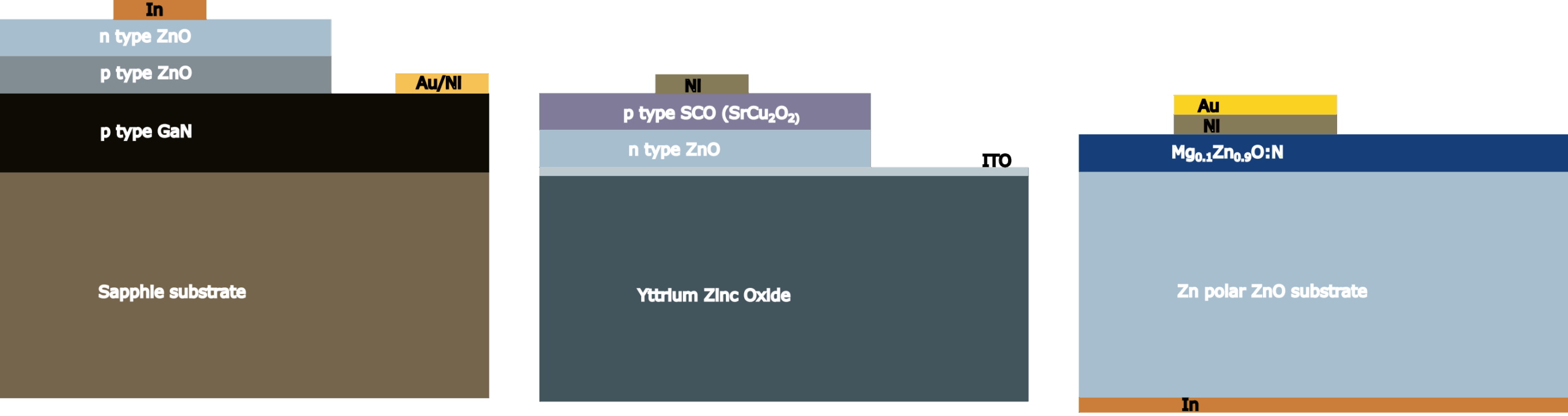
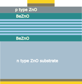
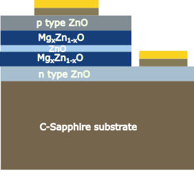
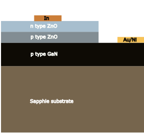
ZnO LEDs come in various structures. We can distinguish two main groups. The single crystal group and the nanoparticle group. Most single Crystal ZnO devices published are heterojunction devices because of the difficulty in making P doped ZnO, but also to confine electron and holes in the same spot for higher efficiency. In heterojunction devices, it was observed that most often, light is emitted by the non Zn0 element, which considerably reduces the interest of making a ZnO device.
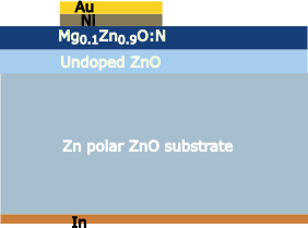
The P type ZnO challenge
In a nutshell: the reasons it is so difficult to get P type ZnO come from the fact that any defect in the crystal missing oxygen in the crystal structure (oxygen vacancy) excess of Zn in the crystal (zinc interstitial) result in the an excess electron that compensate for any hole we manage to introduce. To be exact Zn vacancy and oxygen interstitial exist but they are out numbered in most growth conditions.
Unstable: An important issue is that P doped ZnO is not very stable. In certain conditions such as high temperature strong light irradiation, the hole conduction effect wears off progressively. This means also that the doping processes are not very reproducible as many factors might counter the P doping effect.
Most ions needed for p type doping have a low solubility in ZnO. This means that we cannot put high level of these ions as part of the crystal structure, they will stay either interstitial or disorganize the crystal structure.
Inefficient dopants: Like most wide band gap semiconductors the P acceptor levels tend to be deep in the band gap. In other words it take significant energy to get a valence band electron to hop into an acceptor level. The consequence is that not all the dopant inserted are active increasing the required concentration needed for a set value of doping.
That said, there has been recent success in achieving p doping of ZnO. Several new ways have been successful. Phosphor is a P type dopant for ZnO and one of the simplest ways of doping ZnO is to form a P source using a spin on dopant on a silicon wafer and annealing in oxygen. This forms a Phosphorous rich glass on top of the Si wafer. This wafer becomes a source of phosphorous when it heated in oxygen in very close proximity with a ZnO layer[1]. More advanced techniques such as ion implantation are also used with P [2]. Li doping using electrolysis. Nitrogen doping during molecular beam epitaxy, Cu, Ag or Au under oxygen rich conditions seem to result in more stable P doped ZnO.
Co-doping: doping of two different elements has been shown[1,2] as a valid way to increase solubility of dopants. That is the case for Ga[3] or Al [4] to achieve more N doping All these tend to show that it is a matter of time before we start seeing more competitive ZnO LEDs being made and why not in the market.
[1]Mishra, Madhuri, et al. "Phosphorus doping of ZnO using spin‐on dopant process: A better choice than costly and destructive ion-implantation technique." Journal of Luminescence 233 (2021) https://doi.org/10.1016/j.jlumin.2021.117921

[2] Lu,J.; Ye, Z.; Zhuge, F.; Zeng, Y.; Zhao, B.; Zhu, L. p-type conduction in N–Al co-doped ZnO thin films. Appl. Phys. Lett. 2004, 85, 3134–3135. https://pmc.ncbi.nlm.nih.gov/articles/PMC11243417/

[3]Tsay, C. Y., & Chiu, W. Y. (2020). Enhanced electrical properties and stability of p-type conduction in zno transparent semiconductor thin films by co-doping ga and n. Coatings, 10(11), 1069.
 https://doi.org/10.3390/coatings10111069

[4] Xiang, Y., Tang, H., Zhu, Z., Pang, B., Zhou, T., Zhan, H., ... & Zhou, Y. (2024). First‐Principles Study of the Al–N‐Codoped Zincblende ZnO. physica status solidi (RRL)–Rapid Research Letters, 18(11), 2400104.
 https://doi.org/10.1002/pssr.202400104

Leave a Reply