

When electron are confined in a very narrow space, their energy is quantized. This means that in the valence or the conduction band they can only take discrete energy levels. Many of such quantum structures called quantum wells can be fabricated side by side, forming multi quantum well structures.
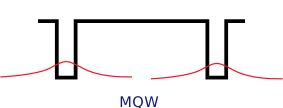
The electron wave function in a real device extends beyond the limits (walls) on the quantum well. This means that there is a non-zero probability to find the electron out of the well. Therefore if the wells are very close the electron can tunnel (move) form one well to the next provided that the allowed energy levels align.

When the wells are extremely close, electrons wave functions overlap and therefore, following Pauli’s exclusion principle new energy levels appear. These new energy levels forms bands in the super lattice.
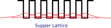

These are generally fabricated using Molecular Beam Epitaxy. However new methods are being developed such as the stacking of 2D semiconductor materials. This can be achieved using materials couples such as MoS2/WSe
Types of super lattices
Hetero junction superlattices. In this case two materials of different bandgaps are deposited sequentially to obtain the desired structure.
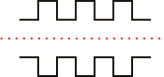
Using Epitaxially grown doped homojunction layers one can achieve similar results quantum wells. These structure are called nini structures as they alternate n doped and intrinsic layers
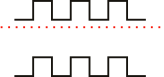
Inter Sub-band components
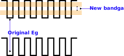
They enable the fabrication of microelectronic component that need:
- Very small bandgaps
- small bandgap in optically transparent materials
- small bandgap while benefitting of some wider bandgaps materials properties

Leave a Reply